74LVC1GX04
One chip crystal oscillator driver
Features
·
+ / - 24 mA output drive
·
Multiple package options
·
Wide supply voltage range 1.65 to 5.5 volts
·
Wide operating temperature range -40 to +125ºC
·
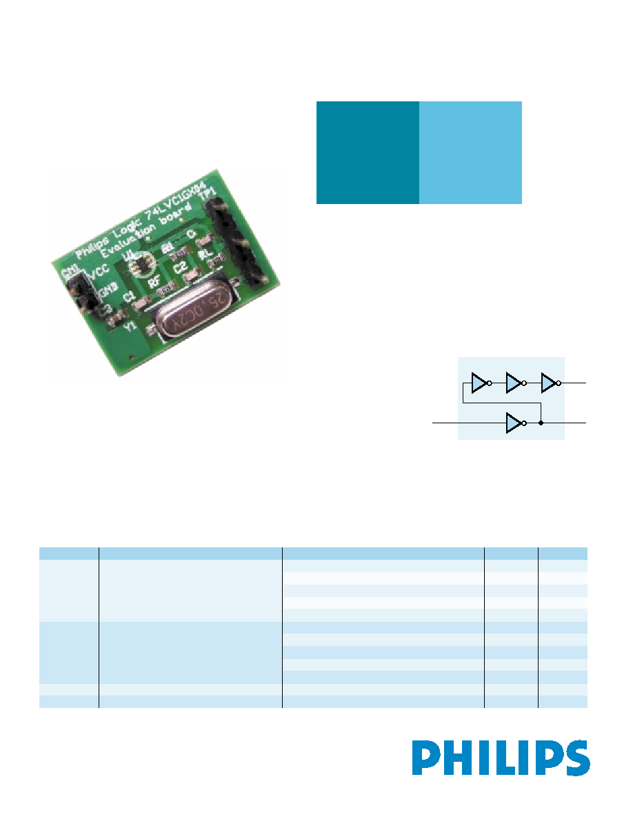
Demo board available
·
Isolation of the Crystal from system loading
·
Astable Multivibrator
Description
The 74LVC1GX04 combines the functions of the 74LVC1GU04 and
74LVC1G04 into a single package to provide a device optimized for use
in crystal oscillator applications. This integration produces the benefits of
a compact footprint, lower power dissipation, and stable operation over a
wide range of frequency and temperature.
The device is fully specified for partial power-down applications using I
off
at
output Y. This disables the output, preventing damaging backflow current
when the device is powered down.
Applications
·
Crystal Oscillator
·
Astable Multivibrator
Benefits
·
Single chip
·
Low Power
·
Optimized design can be
reused regardless of system load
S e m i c o n d u c t o r s
Symbol
Parameter Conditions
Typical
Unit
t
PHL
/t
PLH
propagation delay input X1 to output X2
V
CC
= 1.8 V; C
L
= 30 pF; R
L
= 1 k
2.1
ns
V
CC
= 2.5 V; C
L
= 30 pF; R
L
= 500
1.7
ns
V
CC
= 2.7 V; C
L
= 50 pF; R
L
= 500
2.5
ns
V
CC
= 3.3 V; C
L
= 50 pF; R
L
= 500
2.1
ns
V
CC
= 5.0 V; C
L
= 50 pF; R
L
= 500
1.6
ns
t
PHL
/t
PLH
propagation delay input X1 to output Y
V
CC
= 1.8 V; C
L
= 30 pF; R
L
= 1 k
4.1
ns
V
CC
= 2.5 V; C
L
= 30 pF; R
L
= 500
2.9
ns
V
CC
= 2.7 V; C
L
= 50 pF; R
L
= 500
3.0
ns
V
CC
= 3.3 V; C
L
= 50 pF; R
L
= 500
2.8
ns
V
CC
= 5.0 V; C
L
= 50 pF; R
L
= 500
2.3
ns
C
I
input capacitance
5
pF
C
PD
power dissipation capacitance per buffer
output enabled
35
pF
Quick reference data
GND = 0 V; T
amb
= 25°C
LVC1GX04
n.c.
X1
Y
X2
6
4
1
3
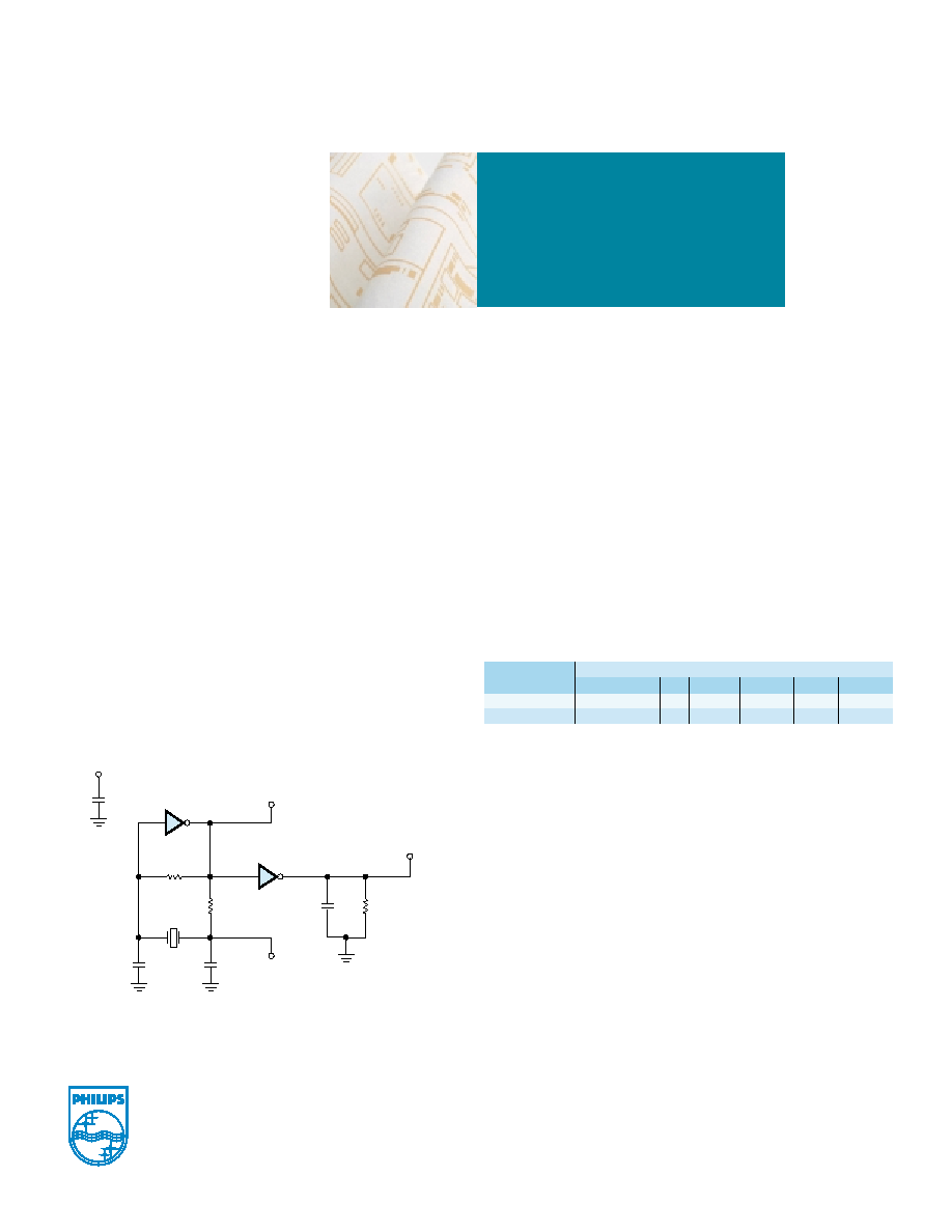
In designing a crystal oscillator, the values of C
1
and C
2
as shown in the
reference design are dependent on the selected crystal. R
1
is critical to the
start up performance and drive level to the crystal. Because the system load
is isolated by the internal buffer in the 74LVC1GX04, these calculations can
be done once for many different system loads. For the reference design as
shown, the crystal load capacitance (C
L
) should be equal to the capacitance
C
1
and C
2
in parallel in addition to any stray capacitance (C
s
)
C
1
and C
2
should be equal and the designer can use the following formula
to calculate the value:
C
L
= (C
1
*C
2
) / (C
1
+C
2
) +C
s
Where:
C
L
is the load capacitance as specified by the crystal manufacturer, C
s
is the
stray capacitance of the circuit which is equal to the input capacitance of the
74LVC1GX04 of 5 pF. The feedback resistor (R
f
) provides negative feedback
and sets a bias point for the un-buffered inverter. This value is not critical
and is typically 1 Meg.
The starting value for R
1
should be equal to the reactance of C
2
at the
crystal frequency. (R
1
= X
C2
)
This will result in an input to the crystal of 50% of the rail to rail output
of X2. Usually this keeps the drive level into the crystal within the drive
specifications of the crystal but the designer should verify this. Overdriving
the crystal can cause damage.
After the calculations are performed for a particular crystal, the oscillator
circuit should be tested. The following simple checks will verify the
prototype design of a crystal controlled oscillator:
·
Test the oscillator over worse case conditions of min-max operating
voltage and temperature.You can also simulate worse case crystal
variations by adding series and parallel resistors.
·
Insure that the circuit does not oscillate when the crystal is removed.
·
Check the frequency stability over a supply range slightly greater than
which is likely to occur during normal operation.
·
Check that the start up time is within system requirements.
74LVC1GX04
One chip crystal oscillator driver
w w w . s e m i c o n d u c t o r s . p h i l i p s . c o m
P h i l i p s S e m i c o n d u c t o r s
Philips Semiconductors is a worldwide company with over 100 sales offices
in more than 50 countries. For a complete up-to-date list of our sales offices
please e-mail sales.addresses@www.semiconductors.philips.com.
A complete list will be sent to you automatically. You can also visit our
website http://www.semiconductors.philips.com/sales
© Koninklijke Philips Electronics N.V. 2003
All rights reserved. Reproduction in whole or in part is prohibited without the prior written consent
of the copyright owner.The information presented in this document does not form part of any quo-
tation or contract, is believed to be accurate and reliable and may be changed without notice. No lia-
bility will be accepted by the publisher for any consequence of its use. Publication thereof does not
convey nor imply any license under patent- or other industrial or intellectual property rights.
Date of release: August 2003
document order number: 9397 750 11958
Published in U.S.A.
www.semiconductors.philips.com/logic
Packages
Part Number
Temp. Range Pins Package Material
Code
Marking
74LVC1GX04GW -40º to +125º C
6
SC-88
plastic
SOT363
VX
74LVC1GX04GV
-40º to +125º C
6
SC-74
plastic
SOT457
VX4
Ordering information
Evaluation Board reference design schematic
C3
0.1
µF
C2
22P
CL
22P
R1
330
RL
500
CL
50P
V
CC
U1A
U1B
Rf
74LVC1G04GW
X1
Citizen
HCM49
74LVC1G04GW
1M
6
4
1
1
3
TP1
Test Point A
TP2
Test Point B
TP3
Test Point C